Advanced Packaging Materials for Semiconductors Market – Analysis and Forecast (2025-2030)
Industry Insight by Material Type (silicones, copper, low-k dielectric, mold compounds, BT Resin (Bismaleimide Triazine), glass interposers, and solder Materials), by Packaging Platform (Flip Chip, Embedded Die, Fan-in Wafer Level Packaging, and Fan-out Wafer Level Packaging (FOWLP)), by End-User (automobile, electrical and electronics, power and energy, and other industries), and Geography (U.S., Canada, Germany, U.K., France, China, Japan, India, and Rest of the World)
| Status : Published | Published On : Jan, 2024 | Report Code : VRSME9146 | Industry : Semiconductor & Electronics | Available Format :

|
Page : 202 |
Advanced Packaging Materials for Semiconductors Market – Analysis and Forecast (2025-2030)
Industry Insight by Material Type (silicones, copper, low-k dielectric, mold compounds, BT Resin (Bismaleimide Triazine), glass interposers, and solder Materials), by Packaging Platform (Flip Chip, Embedded Die, Fan-in Wafer Level Packaging, and Fan-out Wafer Level Packaging (FOWLP)), by End-User (automobile, electrical and electronics, power and energy, and other industries), and Geography (U.S., Canada, Germany, U.K., France, China, Japan, India, and Rest of the World)
Advanced Packaging Materials for Semiconductors Market Overview
Advanced Packaging Materials for Semiconductors are a range of specialized substances used in assembling and protecting semiconductor components. These materials are designed to fulfill demanding performance standards. Preferred for their insulating qualities and thermal stability, silicones help with efficient heat management, while high conductivity copper is preferred for interconnects, low-k dielectrics for minimized signal distortion. In fan-out wafer-level packaging (FOWLP), mold compounds provide mechanical durability. Ingenious materials like glass interposers allow 3D stacking for more integration, while organic substrates like BT resin improve interconnect density.
Global Advanced Packaging Materials for Semiconductors market was worth USD 34.29 billion in 2023 and is expected reach USD 59.00 billion by 2030 with a CAGR of 7.02% during the forecast period, i.e., 2025-2030. The growing demand for advanced packaging materials is driven by the rising semiconductor complexity, demand for miniaturization, and higher processing speeds. Additionally, thermal management, power efficiency, and 3D integration capabilities are driving the demand for specialized packaging solutions for semiconductors.
Geographically, the market is expanding rapidly in North America, Europe, and the Asia Pacific, as a result of the presence of large companies such as Taiwan Semiconductor Manufacturing Company (TSMC), Intel Corporation, and Advanced Semiconductor Engineering, Inc. (ASE Group), huge investment in the R&D, and growing demand for EVs; however, the market confronts constraints such as investment requirement and adverse economic environment. Overall, the Advanced Packaging Materials for Semiconductors market offers potential prospects for market participants to develop and fulfill the growing needs of wide range of industries including automobile, electrical and electronics, power and energy, and other industries.
Advanced Packaging Materials for Semiconductors Market Segmentation
Insight by Material Type
Based on the material type, the global Advanced Packaging Materials for Semiconductors market is segmented into silicones, copper, low-k dielectric, mold compounds, BT Resin (Bismaleimide Triazine), glass interposers, and solder Materials. Copper dominated the global Advanced Packaging Materials for Semiconductors market with ~40% share in 2023 due to its excellent electrical conductivity, which is essential for effective data transfer inside chips. Its high thermal conductivity also aids in effective heat dissipation, vital for maintaining optimal operating temperatures in high-performance devices. Copper is a seamless option for interconnects due to its compatibility with semiconductor fabrication methods. Its affordability and plentiful availability also contribute to its dominant share in the market. Furthermore, Copper's dominant position in the semiconductor packaging business is cemented by the growing need for faster and more powerful chips resulting from advancements in semiconductor technologies.
Insight by Packaging Platform
Based on the packaging platform, the global Advanced Packaging Materials for Semiconductors market is segmented into Flip Chip, Embedded Die, Fan-in Wafer Level Packaging, and Fan-out Wafer Level Packaging (FOWLP). In 2023, FOWLP dominated the global Advanced Packaging Materials for Semiconductors market as it allows several dies to be stacked and coupled on a single substrate, providing improved integration capabilities. Its superior electrical performance, small size, and ability to dissipate heat make it appropriate for a variety of uses, from high-performance computing to mobile electronics. Furthermore, FOWLP allows for a smaller form factor and enhances signal integrity, which makes it a flexible option for contemporary semiconductor packaging requirements. This adaptable platform's outstanding performance and efficiency advantages have helped it gain the dominant share in the Advanced Packaging Materials for Semiconductors market.
Insight by End-User
Based on the end-use industry, the global Advanced Packaging Materials for Semiconductors market is segmented into automobile, electrical and electronics, power and energy, and other industries. The electrical and electronics industry dominated the market in 2023 owing to its wide range of applications. Modern electronics are built on semiconductors, which are used to power everything from industrial machines to cellphones and advanced packaging materials are becoming more and more necessary as customer demands for quicker, smaller, and more energy-efficient electronics rise. The industry's growing demand for high-performance semiconductors fuels ongoing packaging material innovation. Furthermore, the electrical and electronics industry's dominance in the global Advanced Packaging Materials for Semiconductors market is cemented by the strict quality and reliability standards in industries like aerospace and healthcare, which demand state-of-the-art packaging materials to protect delicate electronic components.
Global Advanced Packaging Materials for Semiconductors Market Report Coverage
|
Report Metric |
Details |
|
Historical Period |
2020 - 2024 |
|
Base Year Considered |
2025 |
|
Forecast Period |
2026 - 2035 |
|
Market Size in 2025 |
U.S.D. 34.29 Billion |
|
Revenue Forecast in 2035 |
U.S.D. 59.00 Billion |
|
Growth Rate |
7.02% |
|
Segments Covered in the Report |
By Material Type, By Packaging Platform, and By End-User |
|
Report Scope |
Market Trends, Drivers, and Restraints; Revenue Estimation and Forecast; Segmentation Analysis; Companies’ Strategic Developments; Market Share Analysis of Key Players; Company Profiling |
|
Regions Covered in the Report |
North America, Europe, Asia-Pacific, Middle East, and Rest of the World |
Industry Dynamics
Advanced Packaging Materials for Semiconductors Market Growth Drivers
Growing demand for electric vehicles
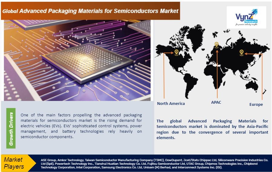
One of the main factors propelling the advanced packaging materials for semiconductors market is the rising demand for electric vehicles (EVs). EVs' sophisticated control systems, power management, and battery technologies rely heavily on semiconductor components. Silicones, highly valued for their superior thermal conductivity, are essential for effectively dispersing the heat produced by the powerful electric drivetrains. Because of its high conductivity, copper is used for interconnects in the EVs, which guarantees effective signal transmission in the control systems of the car. In order to maximize the performance of EVs, low-k dielectrics are essential for cutting down on energy consumption and signal delays.
The EV's engine and control systems' delicate electronic components are mechanically protected by mold compounds while organic substrates employ BT Resin (Bismaleimide Triazine), which increases interconnect density and permits compact designs. Furthermore, solder materials are essential for connecting and bonding different semiconductor components in electric vehicles (EVs), resulting in strong and dependable electrical connections. The development of the semiconductor packaging business is fueled by the combined effects of these advanced packaging materials, which help semiconductor devices in electric vehicles operate dependably and efficiently.
Emergence of Internet of Things (IoT)
The Internet of Things' (IoT) rapid proliferation is a major growth driver for the advanced packaging materials for semiconductors market. Compact, high-performance semiconductor packages are becoming more and more in demand as a result of the widespread use of sensors and linked devices across numerous industries. Specialized packaging materials that combine reliability, miniaturization potential, and thermal stability are needed for IoT applications.
Key players in semiconductor manufacturing and packaging services, such as ASE Group and Amkor Technology, are at the forefront of satisfying this need. Amkor Technology is a top supplier of test and packaging services for semiconductors. They make significant investments in R&D to provide cutting-edge packaging solutions made specifically for Internet of Things devices. Additionally, major semiconductor foundries like Taiwan Semiconductor Manufacturing Company (TSMC) are also actively involved in developing cutting-edge packaging technologies to support the burgeoning IoT market. These companies are driving innovation in advanced packaging materials to meet the unique requirements of IoT applications, thereby fueling the growth of the advanced packaging materials for semiconductors market.
Advanced Packaging Materials for Semiconductors Market Challenge
Lack of options for advanced packaging materials
The growing need for materials that can withstand the harsh operating conditions is one of the main obstacles for the growth of the advanced packaging materials for semiconductors market. Semiconductor devices produce more heat as they get smaller and more powerful and packaging materials that may efficiently disperse heat without sacrificing structural integrity are in high demand. One of the biggest challenges faced by the businesses is finding the materials that properly balance electrical insulation, mechanical toughness, and thermal conductivity. The production of such sophisticated packaging materials is major roadblock in the advancement of semiconductor technology.
Advanced Packaging Materials for Semiconductors Market Geographic Overview
- North America
- Europe
- Asia Pacific (APAC)
- Middle East and Africa (MEA)
- South America
The global Advanced Packaging Materials for Semiconductors market is segmented into North America, Europe, the Asia-Pacific, Latin America, and the Middle East and Africa region. The global Advanced Packaging Materials for Semiconductors market is dominated by the Asia-Pacific region due to the convergence of several important elements. Notably, it is home to epicenters for semiconductor production, such as South Korea, China, and Taiwan, all of which have highly developed manufacturing capacities. The headquarters of prominent players including Samsung Electronics, Amkor Technology, and ASE Group propel innovation in packaging technology.
Additionally, the market's expansion is supported by strategic alliances between local businesses and international material suppliers, such as ASE's alliance with Henkel. Key roles are played by government programs that support R&D and infrastructure expenditures in semiconductor businesses, such as Taiwan's "Asian Silicon Valley" project. Asia-Pacific is a pioneer in innovative semiconductor packaging materials owing to its strong ecosystem, which combines technological know-how, strategic alliances, and supportive regulations.
Competitive Insight
One of the leading companies in the advanced packaging materials for semiconductors market is Taiwan Semiconductor Manufacturing Company (TSMC). TSMC is well-known for its foundry services, but it also has a significant presence in packaging technology. Their cutting-edge InFO (Integrated Fan-Out) packaging technology makes it possible to create small, powerful chips. TSMC's dedication to innovation is demonstrated by its partnerships with sophisticated packaging companies such as ASE (sophisticated Semiconductor Engineering) and material suppliers like Dow. TSMC is at the forefront of semiconductor developments, setting industry standards for performance, miniaturization, and power efficiency through strategic partnerships and state-of-the-art packaging processes.
ASE Group holds a prominent position within the advanced packaging materials for semiconductors market. ASE has alliances with top producer of electronics components, such as TDK Corporation, and works closely with material suppliers like Henkel. Industry recognition has been awarded to ASE for its vast knowledge of flip-chip packaging and System-in-Package (SiP) solutions. Furthermore, Universal Scientific Industrial (USI), a subsidiary of ASE Group, expands the group's system integration capabilities. ASE remains a powerful force in the semiconductor packaging industry due to its solid relationships across the supply chain and a wide range of packaging techniques.
Recent Development by Key Players
In September 2023, Samsung announced that it is automating its semiconductor packaging with initial results showing doubled efficiency. Samsung has become the first company in the world to launch a labor-free semiconductor packaging line with a goal of converting its packaging plants to be human labor-free by 2030.
In September 2023, the Electronics and Telecommunications Research Institute (ETRI) in South Korea developed a revolutionary 95% power-saving semiconductor packaging technology, marking the first time such an advancement has been accomplished. The new process has streamlined the semiconductor chiplet packaging process from a complex nine-step procedure to just three simple steps.
Key Players Covered in the Report
ASE Group, Amkor Technology, Taiwan Semiconductor Manufacturing Company (TSMC), DowDupont, Jcet/Stats Chippac Ltd, Siliconware Precision Industries Co. Ltd (Spil), Powertech Technology Inc., Tianshui Huatian Technology Co. Ltd, Fujitsu Semiconductor Ltd, UTAC Group, Chipmos Technologies Inc., Chipbond Technology Corporation, Intel Corporation, Samsung Electronics Co. Ltd, Unisem (M) Berhad, and Interconnect Systems Inc. (ISI).
The Advanced Packaging Materials for Semiconductors market report offers a comprehensive market segmentation analysis along with an estimation for the forecast period 2025–2030.
Segments Covered in the Report
By Material Type
- Silicones
- Copper
- Low-k Dielectric
- Mold Compounds
- BT Resin (Bismaleimide Triazine)
- Glass Interposers
- Solder Materials
By Packaging Platform
- Flip Chip
- Embedded Die
- Fan-in Wafer Level Packaging
- Fan-out Wafer Level Packaging (FOWLP)
By End-Use Industry
- Automotive Industry
- Electrical and Electronics Industry
- Power and Energy Industry
- Other End-use Industry
Region Covered in the Report
North America
- U.S.
- Canada
- Mexico
Europe
- Germany
- U.K.
- France
- Italy
- Spain
- Russia
- Rest of Europe
Asia-Pacific (APAC)
- China
- Japan
- India
- South Korea
- Rest of Asia-Pacific
Middle East and Africa (MEA)
- Saudi Arabia
- U.A.E
- South Africa
- Rest of MEA
South America
- Argentina
- Brazil
- Chile
- Rest of Latin America
Primary Research Interviews Breakdown
%20System%20Market.png "France Skincare Devices Market Size")
Frequently Asked Questions
Purchase Options
Latest Report
Research Methodology
- Desk Research / Pilot Interviews
- Build Market Size Model
- Research and Analysis
- Final Deliverable
Connect With Our Sales Team
- Toll-Free: 1 888 253 3960
- Phone: +91 9960 288 381
- Email: enquiry@vynzresearch.com
Advanced Packaging Materials for Semiconductors Market