Advanced Semiconductor Packaging Market Size & Share - Growth Forecast Report (2026-2035)
Industry Insight by Packaging Type (Fan Out Wafer-Level Packaging (FO-WLP), Flip-Chip Packaging, 2.5D/3D Packaging), by Application (Consumer Electronics, Automotive, Telecommunication, Industrial, Aerospace and Defense, Healthcare, Others), by End User (Outsourced Semiconductor Assembly and Test (OSAT) Providers, Integrated Device Manufacturers (IDMs), Foundries, Automotive Manufacturers, Others)
| Status : Published | Published On : Mar, 2026 | Report Code : VRSME9198 | Industry : Semiconductor & Electronics | Available Format :
|
Page : 195 |
Advanced Semiconductor Packaging Market Overview
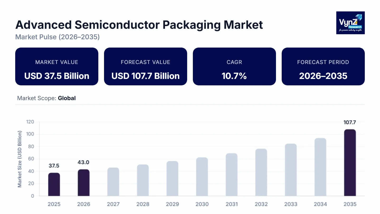
The advanced semiconductor packaging market which was valued at approximately USD 37.5 billion in 2025 and is estimated to reach around USD 43.0 billion in 2026, is projected to reach close to USD 107.7 billion by 2035, expanding at a CAGR of about 10.7% during the forecast period from 2026 to 2035.
The market is entering a decisive growth phase as the industry confronts the physical and economic limits of traditional chip scaling. Performance gains today are no longer driven solely by smaller transistors, but by how intelligently chips are integrated, connected, and optimized at the package level. Technologies such as fan-out, 2.5D, and 3D packaging enable higher computing density, faster data movement, improved power efficiency, and compact form factors—capabilities that are essential for artificial intelligence, high-performance computing, automotive electronics, and next-generation communication systems.
At the same time, advanced packaging has evolved from a backend manufacturing step into a strategic differentiator. Chiplet-based architectures allow companies to combine heterogeneous dies, reuse proven designs, manage costs, and accelerate time-to-market without relying exclusively on leading-edge nodes. This shift is redefining value creation across the semiconductor ecosystem, elevating the role of OSAT providers, strengthening foundry–customer collaboration, and opening new investment pathways for regions building domestic semiconductor capabilities.
Policy-driven ecosystem development is further amplifying market momentum. In India, the India Semiconductor Mission under the Semicon India Programme has introduced a ₹76,000 crore incentive framework to catalyze the sector. As of late 2025, ten approved projects—spanning fabs, advanced packaging, OSAT, and memory units—represent cumulative envisaged investments of ₹1.60 lakh crore (approximately USD 19 billion) across six states, with several facilities already progressing toward pilot production. This underscores how advanced packaging is often the fastest and most scalable entry point into semiconductor manufacturing.
Together, rising technology complexity, supply-chain realignment, and decisive government support are positioning advanced semiconductor packaging as one of the most critical and high-growth segments of the global semiconductor industry—making it a compelling focus for forward-looking enterprises and investors alike.
Advanced Semiconductor Packaging Market Dynamics
Market Trends
The Advanced semiconductor packaging market is witnessing a profound shift toward heterogeneous integration, where diverse chiplets from multiple process nodes are seamlessly combined within a single package to achieve superior performance, power efficiency, and scalability. This trend is revolutionizing high-performance computing and AI applications by enabling modular designs that reduce time-to-market and costs. As devices demand more from limited space, innovations like 2.5D interposers and 3D stacking with through-silicon vias are becoming standard, fostering collaborations between foundries and OSAT providers. In the United States, the CHIPS National Advanced Packaging Manufacturing Program finalized $300 million in awards in 2025 to advance substrates and materials, bolstering domestic innovation. This evolution not only addresses the end of Moore's Law scaling but also empowers industries like telecommunications and automotive to deploy edge AI solutions. For CEOs eyeing long-term dominance, embracing heterogeneous integration means unlocking unprecedented system-level optimizations, positioning your enterprise at the forefront of a market transforming global technology landscapes through smarter, more adaptive semiconductor architectures.
Growth Drivers
The primary driver of the advanced semiconductor packaging market is the accelerating demand for high-performance, intelligent, and connected systems. Applications such as artificial intelligence, autonomous and electric vehicles, telecommunications infrastructure, and industrial automation require faster data processing, lower latency, and improved energy efficiency. Advanced packaging technologies address these requirements by enabling dense integration of multiple functional components, reducing signal loss and improving thermal performance. Unlike conventional packaging, advanced solutions support customized architectures that align closely with application-specific needs. This capability is critical as product complexity increases and time-to-market pressures intensify. Additionally, the ability to integrate heterogeneous components within a single package allows manufacturers to optimize cost and performance simultaneously. As end markets continue to prioritize computational efficiency and reliability, advanced semiconductor packaging is emerging as a key driver of differentiation and sustained demand across the global electronics ecosystem.
Market Restraints / Challenges
Despite strong growth prospects, the advanced semiconductor packaging market faces challenges related to technical complexity and ecosystem readiness. Advanced packaging processes demand extreme precision, advanced materials, and tightly controlled manufacturing environments. Managing yield, ensuring long-term reliability, and addressing thermal constraints become increasingly difficult as integration density rises. These challenges are further amplified by the need for specialized equipment and highly skilled engineering talent. For new and expanding markets, building a complete ecosystem that spans design, materials, manufacturing, and testing requires coordinated investment and long-term commitment. Any gaps in capability or alignment can slow commercialization and increase operational risk. As advanced packaging becomes more central to product performance, companies must navigate these complexities carefully to ensure scalability, quality, and cost competitiveness. Overcoming these challenges will be critical to unlocking the full potential of advanced semiconductor packaging technologies.
Market Opportunities
The advanced semiconductor packaging market presents a golden opportunity in sustainability-driven innovations, where eco-friendly materials and energy-efficient designs can capture emerging demands in green computing and renewable energy sectors. With global regulations pushing for lower carbon footprints, adopting organic substrates and recyclable interposers offers a pathway to differentiate products while meeting ESG goals. This aligns with the rise of AI and IoT, creating niches for customized packaging in medical devices and aerospace. Government support amplifies this: India's 2026 budget allocated ₹1,000 crore for India Semiconductor Mission 2.0, emphasizing research in sustainable semiconductor equipment and materials. Such investments enable breakthroughs in low-power 3D stacking, opening doors to untapped markets. For forward-thinking CEOs, this opportunity means pioneering circular economy models, reducing waste, and boosting profitability through premium green solutions. By leveraging these trends, your organization can lead in responsible innovation, attract ethical investments, and build lasting partnerships in a transformative era—join forces with us to capitalize on this sustainable revolution and drive unparalleled growth.
Global Advanced Semiconductor Packaging Market Report Coverage
|
Report Metric |
Details |
|
Historical Period |
2020 - 2024 |
|
Base Year Considered |
2025 |
|
Forecast Period |
2026 - 2035 |
|
Market Size in 2025 |
USD 37.5 Billion |
|
Revenue Forecast in 2035 |
USD 107.7 Billion |
|
Growth Rate |
10.7% |
|
Segments Covered in the Report |
Packaging Type, Application, End User |
|
Report Scope |
Market Trends, Drivers, and Restraints; Revenue Estimation and Forecast; Segmentation Analysis; Companies’ Strategic Developments; Market Share Analysis of Key Players; Company Profiling |
|
Regions Covered in the Report |
North America, Europe, Asia Pacific, Rest of the World |
|
Key Companies |
Intel Corporation, Samsung Electronics Co., Ltd., Taiwan Semiconductor Manufacturing Company Limited, Advanced Micro Devices, Inc., ASE Technology Holding Co., Ltd., Amkor Technology, STMicroelectronics N.V., Infineon Technologies AG, Micron Technology, Inc., Texas Instruments Incorporated, Broadcom Inc. and NXP Semiconductors N.V. |
|
Customization |
Available upon request |
Advanced Semiconductor Packaging Market Segmentation
By Packaging Type
Flip-chip packaging remains the largest category, with a market share of around 45% in 2025, due to its long-established role in high-volume semiconductor production. It offers proven reliability, excellent electrical performance, and broad compatibility across consumer, automotive, and industrial applications. Its mature manufacturing ecosystem supports high yields and cost efficiency at scale, making it the preferred choice for processors, memory devices, and high-pin-count ICs. Flip-chip continues to dominate in applications where performance consistency, thermal efficiency, and manufacturability are critical. Its widespread adoption across IDMs, foundries, and OSAT providers ensures sustained volume leadership, even as newer packaging technologies gain traction.
2.5D and 3D packaging represent the fastest-growing category with a CAGR of 10.9% in the coming years, as the industry shifts toward heterogeneous integration and chiplet-based architectures. These technologies enable high-density interconnects, reduced latency, and superior power efficiency by integrating multiple dies within a compact footprint. They are increasingly essential for advanced computing, AI accelerators, and data-intensive systems where traditional packaging falls short. As system complexity rises and performance scaling becomes packaging-driven, 2.5D and 3D solutions are rapidly moving from niche adoption to mainstream deployment, fueling strong growth momentum.
By Application
Consumer electronics remain the largest application category, with an estimated market share of 35% in 2025, due to its massive production volumes and continuous demand for compact, high-performance devices. Smartphones, wearables, and computing devices rely heavily on advanced packaging to support miniaturization, power efficiency, and multi-functional integration. High shipment volumes and short product cycles drive consistent adoption of advanced packaging technologies, particularly fan-out and flip-chip solutions. This sustained demand base ensures that consumer electronics continues to account for the largest share of overall advanced semiconductor packaging consumption.
Automotive is the fastest-growing application category, with a CAGR of 11.2% during the forecast period, as vehicles evolve into software-defined, electronics-intensive platforms. Advanced driver assistance systems, electric powertrains, infotainment, and vehicle connectivity require high-reliability, high-performance semiconductor solutions. Advanced packaging supports these needs by enabling robust thermal management, long-term reliability, and compact system integration. As electronic content per vehicle increases and safety standards become more stringent, automotive demand for advanced semiconductor packaging is accelerating faster than any other end-use segment.
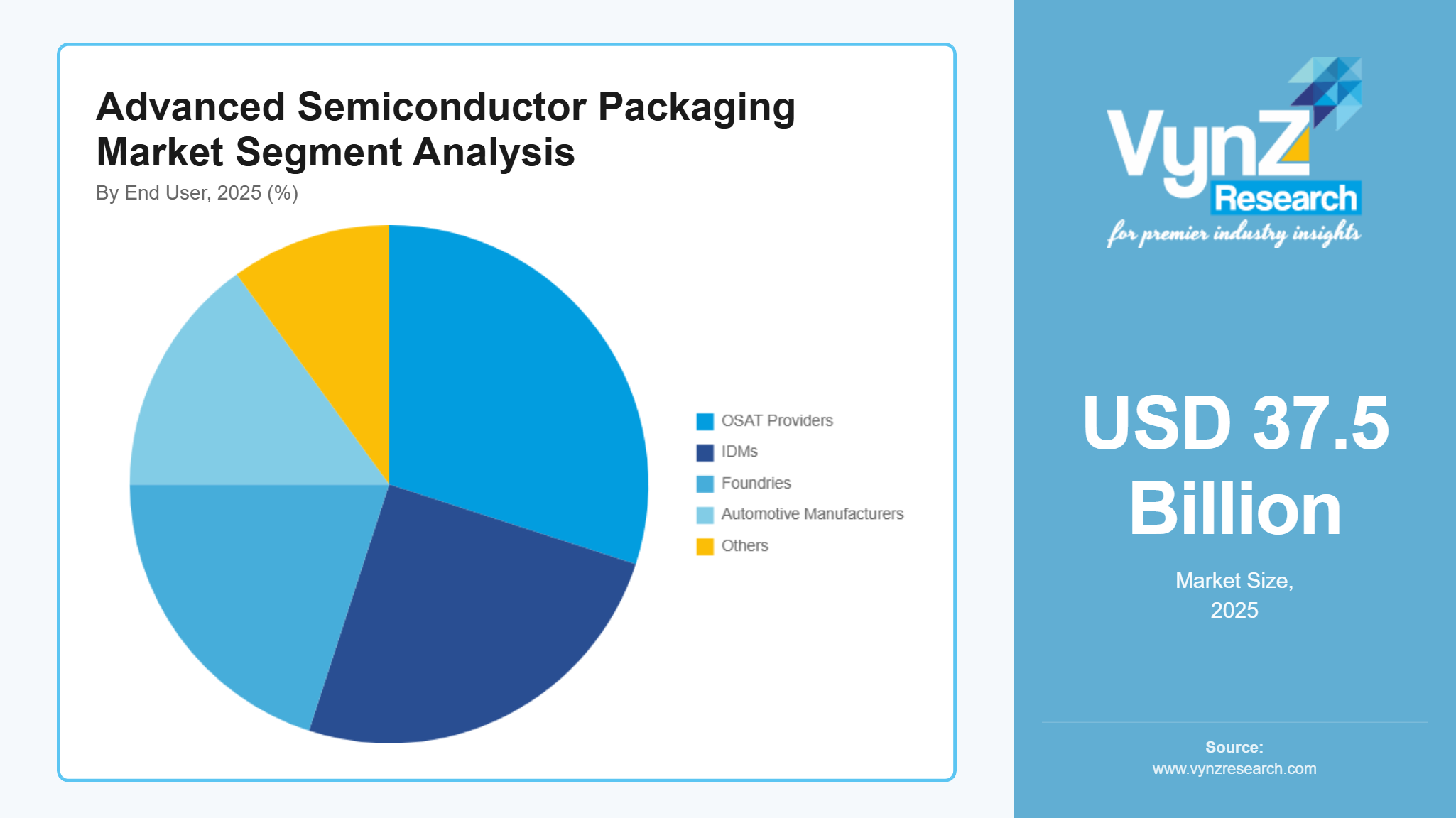
By End User
OSAT providers represent the largest end-user category as advanced packaging increasingly relies on specialized assembly, testing, and integration capabilities. These providers serve a broad customer base, including fabless companies, foundries, and IDMs, enabling high-volume deployment of advanced packaging technologies. Their ability to scale production, optimize yields, and offer cost-effective solutions makes them central to the advanced packaging ecosystem. As complexity increases, reliance on OSAT expertise continues to grow, reinforcing their dominant position.
Foundries are the fastest-growing end-user category as advanced packaging becomes tightly integrated with front-end manufacturing strategies. To support chiplet architectures and system-level optimization, foundries are increasingly offering advanced packaging solutions alongside wafer fabrication. This vertical integration enables better performance tuning, faster time-to-market, and stronger customer lock-in. As packaging and process technologies converge, foundries are rapidly expanding their advanced packaging capabilities, driving accelerated growth in this segment.
Regional Insights
Asia Pacific
Asia Pacific represents the largest regional market for advanced semiconductor packaging, driven by its deep-rooted semiconductor manufacturing ecosystem and strong electronics production base. The region hosts a dense concentration of foundries, OSAT providers, and component suppliers, enabling efficient scaling of advanced packaging technologies such as fan-out, flip-chip, and 2.5D/3D integration. High demand from consumer electronics, automotive electronics, and telecommunications continues to fuel adoption across mature and emerging markets within the region. In addition, Asia Pacific benefits from an established talent pool, integrated supply chains, and manufacturing agility, which together lower production costs and shorten development cycles. As advanced packaging becomes central to performance optimization and heterogeneous integration, Asia Pacific’s end-to-end ecosystem strength ensures its continued dominance in terms of volume and installed capacity.
Europe
Europe’s advanced semiconductor packaging market is shaped by its strong presence in automotive, industrial automation, healthcare, and aerospace applications. The region emphasizes reliability, safety, and long product lifecycles, driving demand for robust packaging solutions that can operate under harsh and regulated environments. Advanced packaging technologies are increasingly adopted to support power electronics, sensor integration, and intelligent control systems. Europe’s focus on sustainability and energy efficiency further aligns with advanced packaging’s ability to optimize performance without relying solely on leading-edge nodes. While the region does not match Asia Pacific in volume, it plays a critical role in high-value and application-specific deployments. Continued investment in semiconductor research, manufacturing resilience, and automotive electrification positions Europe as a strategically important and steadily growing market.
North America
North America is the fastest-growing region in the advanced semiconductor packaging market, supported by rising demand for high-performance computing, artificial intelligence, aerospace, defense, and automotive electronics. The region’s growth is increasingly driven by system-level innovation, where advanced packaging plays a critical role in enabling chiplet architectures, high-bandwidth memory integration, and power-efficient designs. Strong collaboration between technology developers, semiconductor manufacturers, and end-use industries is accelerating the adoption of 2.5D and 3D packaging solutions. Additionally, strategic efforts to strengthen domestic semiconductor capabilities are elevating the importance of advanced packaging as a scalable and flexible manufacturing pathway. As performance requirements grow more complex, North America’s focus on innovation, design leadership, and advanced system integration continues to drive rapid market expansion.
Rest of the World
The rest of the world, including Latin America, the Middle East, and Africa, represents an emerging opportunity zone for advanced semiconductor packaging. These regions are at earlier stages of semiconductor ecosystem development but are increasingly focusing on electronics manufacturing, automotive assembly, telecommunications infrastructure, and industrial modernization. Advanced packaging is gaining attention as a practical entry point into the semiconductor value chain due to its relatively lower capital intensity and faster deployment compared to wafer fabrication. Growing investments in smart infrastructure, mobility, and digital transformation are gradually creating demand for packaged semiconductor solutions.
Competitive Landscape / Company Insights
The advanced semiconductor packaging market is moderately fragmented, characterized by the presence of a mix of global leaders and specialized regional players competing across different technology and application segments. While a few large players command strong positions in high-volume and high-complexity packaging solutions, no single company dominates the entire market. This fragmentation is driven by the diversity of packaging technologies, varying customer requirements, and the need for application-specific customization.
Competition is increasingly centered on technological capability rather than scale alone. Companies differentiate themselves through expertise in fan-out, flip-chip, and advanced 2.5D and 3D packaging, as well as through their ability to deliver high yields, reliability, and rapid time-to-market. Strategic investments in advanced materials, process innovation, and automation are critical factors shaping competitive positioning. Partnerships across the value chain—spanning foundries, OSAT providers, equipment suppliers, and system integrators—are becoming more common as packaging complexity increases.
Geographic expansion and ecosystem integration also play a key role in competitive dynamics, with players aligning manufacturing footprints closer to end markets and emerging semiconductor hubs. As advanced packaging becomes central to system-level performance and product differentiation, competition is expected to intensify, favoring companies that combine technological depth, operational excellence, and long-term customer collaboration.
Mini Profiles
Intel Corporation designs and manufactures advanced semiconductor products that power computing, data center, AI, and connectivity solutions across client, cloud, and edge platforms.
Samsung Electronics Co., Ltd. is a global technology leader providing memory, logic, and semiconductor solutions that support mobile devices, data centers, and advanced computing systems.
Taiwan Semiconductor Manufacturing Company Limited is the world’s leading dedicated semiconductor foundry, offering advanced process and manufacturing technologies to global customers.
Advanced Micro Devices, Inc. develops high-performance computing and adaptive solutions, including processors and accelerators for data center, AI, and embedded applications.
Micron Technology, Inc. provides memory and storage solutions that enable data-driven innovation across computing, automotive, mobile, and industrial markets.
Key Players
- Intel Corporation
- Samsung Electronics Co., Ltd.
- Taiwan Semiconductor Manufacturing Company Limited
- Advanced Micro Devices, Inc.
- ASE Technology Holding Co., Ltd.
- Amkor Technology
- STMicroelectronics N.V.
- Infineon Technologies AG
- Micron Technology, Inc.
- Texas Instruments Incorporated
- Broadcom Inc.
- NXP Semiconductors N.V.
Recent Developments
February 2026 - Prime Minister Narendra Modi inaugurated Micron Technology, Inc.’s semiconductor Assembly, Test, Marking, and Packaging (ATMP) facility in Sanand, Gujarat, marking India’s first commercial semiconductor assembly and test plant and expanding the company’s global footprint in chip packaging and memory production.
February 2026 - Advanced Micro Devices, Inc. (AMD) announced an expanded strategic partnership with Meta Platforms to deploy up to 6 gigawatts of AMD Instinct GPUs over multiple generations. Shipments for the initial gigawatt, powered by custom AMD Instinct MI450-series GPUs, are scheduled to begin in the second half of 2026, supporting Meta's AI infrastructure needs.
December 2025 - Intel Corporation signed a strategic partnership with Tata Electronics to explore manufacturing, assembly, and advanced packaging of Intel products in India, aiming to bolster local semiconductor supply chains and accelerate compute and AI hardware production.
October 2025 - Amkor Technology broke ground on a new semiconductor advanced packaging and test campus in Peoria, Arizona, expanding its total investment to $7 billion. This includes additional cleanroom space and a second greenfield facility, marking the first U.S.-based high-volume advanced packaging site to support growing demand in AI and high-performance computing.
Global Advanced Semiconductor Packaging Market Coverage
Packaging Type Insight and Forecast 2026 - 2035
- Fan Out Wafer-Level Packaging (FO-WLP)
- Flip-Chip Packaging
- D/3D Packaging
Application Insight and Forecast 2026 - 2035
- Consumer Electronics
- Automotive
- Telecommunication
- Industrial
- Aerospace and Defense
- Healthcare
- Others
End User Insight and Forecast 2026 - 2035
- Outsourced Semiconductor Assembly and Test (OSAT) Providers
- Integrated Device Manufacturers (IDMs)
- Foundries
- Automotive Manufacturers
- Others
Global Advanced Semiconductor Packaging Market by Region
- North America
- By Packaging Type
- By Application
- By End User
- By Country - U.S., Canada, Mexico
- Europe
- By Packaging Type
- By Application
- By End User
- By Country - Germany, U.K., France, Italy, Spain, Russia, Rest of Europe
- Asia-Pacific (APAC)
- By Packaging Type
- By Application
- By End User
- By Country - China, Japan, India, South Korea, Vietnam, Thailand, Malaysia, Rest of Asia-Pacific
- Rest of the World (RoW)
- By Packaging Type
- By Application
- By End User
- By Country - Brazil, Saudi Arabia, South Africa, U.A.E., Other Countries
Table of Contents for Advanced Semiconductor Packaging Market Report
1. Research Overview
1.1. The Report Offers
1.2. Market Coverage
1.2.1. By
Packaging Type
1.2.2. By
Application
1.2.3. By
End User
1.3. Research Phases
1.4. Limitations
1.5. Market Methodology
1.5.1. Data Sources
1.5.1.1.
Primary Research
1.5.1.2.
Secondary Research
1.5.2. Methodology
1.5.2.1.
Data Exploration
1.5.2.2.
Forecast Parameters
1.5.2.3.
Data Validation
1.5.2.4.
Assumptions
1.5.3. Study Period & Data Reporting Unit
2. Executive Summary
3. Industry Overview
3.1. Industry Dynamics
3.1.1. Market Growth Drivers
3.1.2. Market Restraints
3.1.3. Key Market Trends
3.1.4. Major Opportunities
3.2. Industry Ecosystem
3.2.1. Porter’s Five Forces Analysis
3.2.2. Recent Development Analysis
3.2.3. Value Chain Analysis
3.3. Competitive Insight
3.3.1. Competitive Position of Industry
Players
3.3.2. Market Attractive Analysis
3.3.3. Market Share Analysis
4. Global Market Estimate and Forecast
4.1. Global Market Overview
4.2. Global Market Estimate and Forecast to 2035
5. Market Segmentation Estimate and Forecast
5.1. By Packaging Type
5.1.1. Fan Out Wafer-Level Packaging (FO-WLP)
5.1.1.1. Market Definition
5.1.1.2. Market Estimation and Forecast to 2035
5.1.2. Flip-Chip Packaging
5.1.2.1. Market Definition
5.1.2.2. Market Estimation and Forecast to 2035
5.1.3. D/3D Packaging
5.1.3.1. Market Definition
5.1.3.2. Market Estimation and Forecast to 2035
5.2. By Application
5.2.1. Consumer Electronics
5.2.1.1. Market Definition
5.2.1.2. Market Estimation and Forecast to 2035
5.2.2. Automotive
5.2.2.1. Market Definition
5.2.2.2. Market Estimation and Forecast to 2035
5.2.3. Telecommunication
5.2.3.1. Market Definition
5.2.3.2. Market Estimation and Forecast to 2035
5.2.4. Industrial
5.2.4.1. Market Definition
5.2.4.2. Market Estimation and Forecast to 2035
5.2.5. Aerospace and Defense
5.2.5.1. Market Definition
5.2.5.2. Market Estimation and Forecast to 2035
5.2.6. Healthcare
5.2.6.1. Market Definition
5.2.6.2. Market Estimation and Forecast to 2035
5.2.7. Others
5.2.7.1. Market Definition
5.2.7.2. Market Estimation and Forecast to 2035
5.3. By End User
5.3.1. Outsourced Semiconductor Assembly and Test (OSAT) Providers
5.3.1.1. Market Definition
5.3.1.2. Market Estimation and Forecast to 2035
5.3.2. Integrated Device Manufacturers (IDMs)
5.3.2.1. Market Definition
5.3.2.2. Market Estimation and Forecast to 2035
5.3.3. Foundries
5.3.3.1. Market Definition
5.3.3.2. Market Estimation and Forecast to 2035
5.3.4. Automotive Manufacturers
5.3.4.1. Market Definition
5.3.4.2. Market Estimation and Forecast to 2035
5.3.5. Others
5.3.5.1. Market Definition
5.3.5.2. Market Estimation and Forecast to 2035
6. North America Market Estimate and Forecast
6.1. By
Packaging Type
6.2. By
Application
6.3. By
End User
6.3.1.
U.S. Market Estimate and Forecast
6.3.2.
Canada Market Estimate and Forecast
6.3.3.
Mexico Market Estimate and Forecast
7. Europe Market Estimate and Forecast
7.1. By
Packaging Type
7.2. By
Application
7.3. By
End User
7.3.1.
Germany Market Estimate and Forecast
7.3.2.
France Market Estimate and Forecast
7.3.3.
U.K. Market Estimate and Forecast
7.3.4.
Italy Market Estimate and Forecast
7.3.5.
Spain Market Estimate and Forecast
7.3.6.
Russia Market Estimate and Forecast
7.3.7.
Rest of Europe Market Estimate and Forecast
8. Asia-Pacific (APAC) Market Estimate and Forecast
8.1. By
Packaging Type
8.2. By
Application
8.3. By
End User
8.3.1.
China Market Estimate and Forecast
8.3.2.
Japan Market Estimate and Forecast
8.3.3.
India Market Estimate and Forecast
8.3.4.
South Korea Market Estimate and Forecast
8.3.5.
Rest of Asia-Pacific Market Estimate and Forecast
9. Rest of the World (RoW) Market Estimate and Forecast
9.1. By
Packaging Type
9.2. By
Application
9.3. By
End User
9.3.1.
Brazil Market Estimate and Forecast
9.3.2.
Saudi Arabia Market Estimate and Forecast
9.3.3.
South Africa Market Estimate and Forecast
9.3.4.
U.A.E. Market Estimate and Forecast
9.3.5.
Other Countries Market Estimate and Forecast
10. Company Profiles
10.1.
Intel Corporation
10.1.1.
Snapshot
10.1.2.
Overview
10.1.3.
Offerings
10.1.4.
Financial
Insight
10.1.5.
Recent
Developments
10.2.
Samsung Electronics Co., Ltd.
10.2.1.
Snapshot
10.2.2.
Overview
10.2.3.
Offerings
10.2.4.
Financial
Insight
10.2.5.
Recent
Developments
10.3.
Taiwan Semiconductor Manufacturing Company Limited
10.3.1.
Snapshot
10.3.2.
Overview
10.3.3.
Offerings
10.3.4.
Financial
Insight
10.3.5.
Recent
Developments
10.4.
Advanced Micro Devices, Inc.
10.4.1.
Snapshot
10.4.2.
Overview
10.4.3.
Offerings
10.4.4.
Financial
Insight
10.4.5.
Recent
Developments
10.5.
ASE Technology Holding Co., Ltd.
10.5.1.
Snapshot
10.5.2.
Overview
10.5.3.
Offerings
10.5.4.
Financial
Insight
10.5.5.
Recent
Developments
10.6.
Amkor Technology
10.6.1.
Snapshot
10.6.2.
Overview
10.6.3.
Offerings
10.6.4.
Financial
Insight
10.6.5.
Recent
Developments
10.7.
STMicroelectronics N.V.
10.7.1.
Snapshot
10.7.2.
Overview
10.7.3.
Offerings
10.7.4.
Financial
Insight
10.7.5.
Recent
Developments
10.8.
Infineon Technologies AG
10.8.1.
Snapshot
10.8.2.
Overview
10.8.3.
Offerings
10.8.4.
Financial
Insight
10.8.5.
Recent
Developments
10.9.
Micron Technology, Inc.
10.9.1.
Snapshot
10.9.2.
Overview
10.9.3.
Offerings
10.9.4.
Financial
Insight
10.9.5.
Recent
Developments
10.10.
Texas Instruments Incorporated
10.10.1.
Snapshot
10.10.2.
Overview
10.10.3.
Offerings
10.10.4.
Financial
Insight
10.10.5.
Recent
Developments
10.11.
Broadcom Inc.
10.11.1.
Snapshot
10.11.2.
Overview
10.11.3.
Offerings
10.11.4.
Financial
Insight
10.11.5.
Recent
Developments
10.12.
NXP Semiconductors N.V.
10.12.1.
Snapshot
10.12.2.
Overview
10.12.3.
Offerings
10.12.4.
Financial
Insight
10.12.5.
Recent
Developments
11. Appendix
11.1. Exchange Rates
11.2. Abbreviations
Note: Financial insight and recent developments of different companies are subject to the availability of information in the secondary domain.
Frequently Asked Questions
Purchase Options
Latest Report
Research Methodology
- Desk Research / Pilot Interviews
- Build Market Size Model
- Research and Analysis
- Final Deliverable
Connect With Our Sales Team
- Toll-Free: +1-888-253-3960
- Phone: +91 9960 288 381
- Email: enquiry@vynzresearch.com
Advanced Semiconductor Packaging Market